| Pin No. | Symbol | I/O | Function | Note |
|---|---|---|---|---|
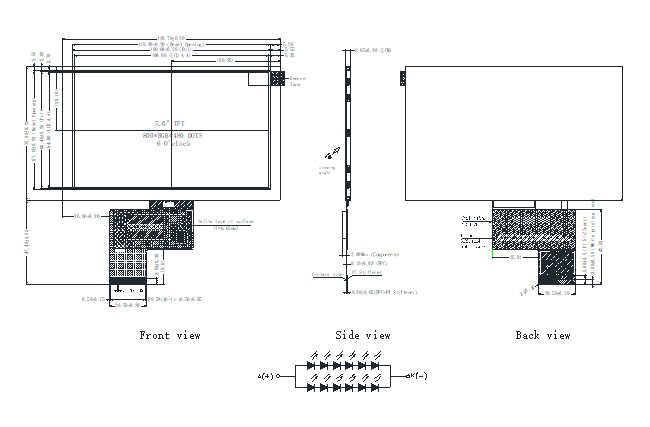
| 1 | VLED- | P | Cathode pin of backlight. | |
| 2 | VLED+ | P | Anode pin of backlight. | |
| 3 | GND | P | Ground. | |
| 4 | VDD | P | Supply voltage(3.3V). | |
| 5-12 | R0-R7 | I | Red data input. | |
| 13-20 | G0-G7 | I | Green data input. | |
| 21-28 | B0-B7 | I | Blue data input. | |
| 29 | GND | P | Ground. | |
| 30 | PCLK | I | Clock signal. Latching data at the rising edge. | |
| 31 | DISP | I | Standby setting for testing, it should be connected to VDD in normal operation mode. If connected to GND, the IC is in standby mode. |
|
| 32 | HSYNC | I | Horizontal Sync input. Negative polarity. |
|
| 33 | VSYNC | I | Vertical Sync input. Negative polarity. | |
| 34 | DE | I | Data input Enable. Active High to enable the data input Bus under "DE Mode". |
|
| 35 | NC | - | No connection. | |
| 36 | GND | P | Ground. | |
| 37 | XR(NC) | A/D | Touch panel Right Glass Terminal. |
|
| 38 | YD(NC) | A/D | Touch panel Bottom Film Terminal. | |
| 39 | XL(NC) | A/D | Touch panel Left Glass Terminal. | |
| 40 | YU(NC) | A/D | Touch panel Top Film Terminal. |
I/O : I: input, O: output, P: power